
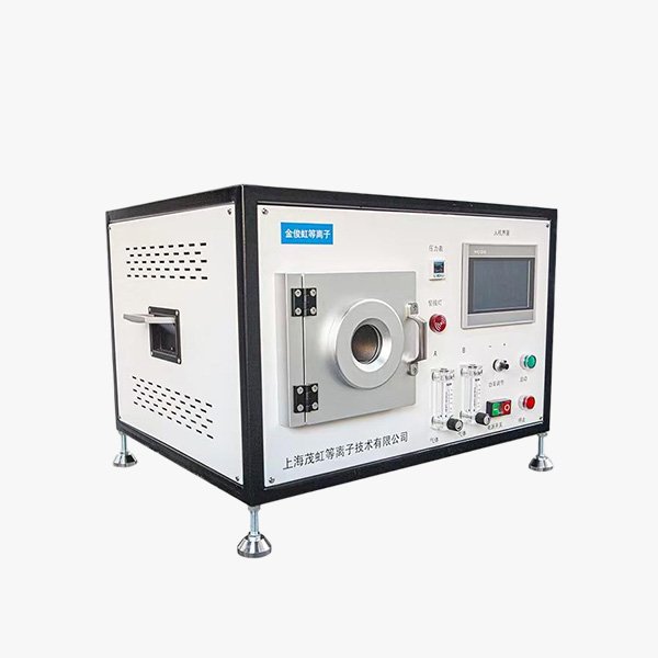
Model: C-XS
Specifications:
Dimensions: 750 × 570 × 450 mm
– Internal chamber volume: 5–30 L
– Electrode and chamber materials: Magnesium-aluminum alloy / SUS304
– Electrode configuration: Horizontal/Vertical
– Plasma output power: 0–1.5 kW (adjustable)
– Power supply frequency: 40 kHz
– Gas inlet/outlet channels: 2 inlets + 1 vent
– Gas flow rate: 0–1000 mL/min (manual adjustment)
– Chamber temperature sensing: None
– Cooling method: Air-cooled
– Discharge vacuum level: 100–500 mTorr
– Compatible gases: Air / O₂ / N₂ / H₂ / CF₄ / Ar / Inert gases
– Applications: 360° multi-faceted treatment of metals, oxides, and polymer materials
Technical Advantages
– Compact desktop design with a small footprint and flexible placement; ideal for laboratories, R&D centers, and small-batch production
– Vacuum chamber processing ensures uniform and stable plasma, delivering consistent and controllable cleaning, activation, and modification results
– Simple user interface with one-touch startup and adjustable parameters; meets the needs of scientific research and process validation
– Gentle processing temperature; compatible with diverse materials; causes no damage to precision samples
– Low power consumption, quiet operation, and easy maintenance; suitable for long-term, frequent use
– High chamber cleanliness; meets requirements for processing high-precision samples in microelectronics, medical, and optical fields
– Supports multiple process gases; enables functions such as cleaning, activation, etching, and photoresist stripping
– Compact size yet stable processing performance; reproducible data facilitates experimental recording and comparison
Solutions
– Provides material surface modification experimental solutions for universities, research institutes, and corporate R&D departments
– Meets needs for new product prototyping, process testing, and small-batch sample pretreatment
– Solves surface cleaning, activation, photoresist stripping, and decontamination issues for tiny precision parts
– Offers high-precision surface treatment solutions for microelectronics, semiconductors, medical consumables, and optical devices – Addresses issues such as poor surface adhesion, weak bonding, printing difficulties, and coating delamination.
– Suitable for a wide range of applications, including laboratory R&D, process validation, sample prototyping, and quality inspection.
Reviews
There are no reviews yet.